

"FAQ"s.... Frequently Asked Questions....
Do, please, feel free to send in your "Q"s, I'll do my best to write "A"s for you, and we'll see how the "F" factor emerges!
Google is all well and good. If you want to find something on this page, don't forget your browser's "find" tool! (Ctrl-F under Firefox, and an edit box appears, lower left.) Also remember that old skool "find" isn't as "smart" as Google's "search".
You will switch back and forth between KiCadHowTo.org and KiCadHowTo.wikidot.com as you follow links in either site. It is spread across the two domains so that I can use the strengths of both to help me build this resource for you. I run both domains; there's nothing "funny" re-directing you.
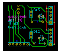
Before we get "to work", if you haven't seen much of KiCad yet, have a quick look at my page with a screenshot of my NoviceGuard PCB, just to see how pretty the KiCad environment is. (The bit at the left is only a limited indication.) Be sure to scroll down to the second image, for an idea of the "quality" of the "cloth". (NoviceGuard is an inexpensive little PCB to let novices use Arduinos easily, and to protect the Arduino from newbie mistakes.)
Where do you start?: Although it is a bit tedious, as it proceeds as if you know nothing, and designs a trivial PCB, I would strongly encourage you to at least skim though the tutorial you'll be taken to if you click on the link in "Where do I start". Besides getting you started with KiCad... which you may already be... it gives you some of the terms and conventions used across KiCadHowTo.
How does the KiCad system for panning and zooming in and out work? In a word: Brilliantly! I now find myself feeling the lack of the KiCad system in other applications I use. The KiCad pan and zoom system may feel a little odd at first, but I think you will like it, once you understand "the trick".
How do you persuade the boss? If you work on a computer that you don't control, you will have to persuade the network administrator to install KiCad. The administrator is in a difficult position. You're going to have to make a good case for taking the risks installing new software entails.
How do you lay down tracks of different widths?
How do you use vias to 'cross' tracks without making them connect?
How do you know the name of an invisible pin? You do care, by the way! For a start, you will need to know the name of an invisible pin which is for a power or ground connection so that you can provide the right power port in the schematic.
Why the weird thing at the top of most pages? Many pages start with something "weird", e.g. "se1pcb2" or "co1lib". What is the reason for that? What is it good for?
How do you back up or clone a project? KiCad does not have an internal tool for this. But it isn't hard. Everyone should do backups from time to time, and many will benefit from being able to use old projects as starting points for new ones.
Having created a design, how do you turn that into an actual board? Doing it yourself.
How do you get your board made by a commercial service? Yes! KiCad "does" Gerber files. (This means that most services won't even know that you were using KiCad... Here's a link to the Wikipedia article on Gerber files for you.)
How can you share schematics and PCB artwork online? The answer? CircuitBee.com. But the full FAQ answer tells you a bit more. Like why CircuitBee is better than PDFs, or the graphic images I've been using... so far... at KiCadHowTo.org!
How do you work with mini-boards? By "mini-board", I just mean an already finished, populated PCB, for instance a breakout board for a W5100 interface. How do you draw a schematic with a reference to that, and how do you carry that forward to a PCB?
How do you import files from the Eagle PCB-CAD world? I haven't got a good answer to that for you yet... but here's a page with as much as I do have for you to date.
How do you maintain a "global" version ID? You should be able to enter a "version ID" string somewhere, but enter it just once, and find that text on every schematic, every PCB, until you next change the version ID string the same way. I haven't (quite) achieved that... but I do have a crude "make-do".
For the FAQs above here, the first bit of each paragraph is a link which takes you to a page dedicated to answering that FAQ. For the FAQs below here, I have not yet written a separate page.
-------------
Is it "connected"?: This is a question that arises in the "draw schematic" phase of the design cycle. Just because two things lie on top of one another, it doesn't mean that they are connected! It may be identified as "Err Type 2". KiCad does a pretty good job of connecting things when it should, and leaving them unconnected otherwise. But it doesn't do a perfect job of reading your mind! You ARE using the ERC tool, aren't you?! (If you get "Pin not connected...", you may well have a case of two things merely lying on top of one another.) To test if two things are connected (when drawing the schematic): Try dragging one of them. (Put cursor on component, press "G", move mouse.) If it pulls away from the thing you thought was connected, they weren't. If the one drags the other, they were!
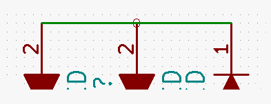
Little circles, as at the top end of the middle diode above, tell you something is not connected to a wire it lies on top of. You could fix a "not connected" like that using by the "place junction" tool. That would change the little circle to a slightly larger green-filled circle.
In related news: Sometimes the ERC tool will complain about a pin on a component that has nothing connected to it because you didn't want to connect anything! Just put a Not-Connected Flag on it to reassure the ERC. Ignoring warnings because you "know" they are "not important" is very risky! (The Not-Connected Flag is available via the blue cross on the eeschema right-hand toolbar). It tells KiCad that you haven't simply forgotten a pin.
And finally, in the "connections" world, there is the whole question of power "ports" and "flags". They are important, but I haven't yet managed to condense my thoughts on these. A long-winded discussion can be found at my pages Power Ports/ Power Flags. Errors in this area may be identified as "Err Type 3".
What about Upgrading, Updating the KiCad I am using? Good idea, almost always. But not a trivial exercise, with KiCad. At least it wasn't, for me, when in Nov 2016 I went from the build (stable) of 2013-7 (which was working well, and which was still the current best when I checked in 2/15), to version "4-0-4" (stable).
I don't mean to complain... I certainly wouldn't want still to be using the first version of... anything. But updates/ upgrades can be easy, or they can be a bit troublesome. I found that, for me, this time, the upgrade process (essentially a "install as if from new") was trying. I TRIED to "preserve" my old installation, and put the new one "alongside" it. Not entirely successful. Whatever you do, make backups of your project folders, and of any .lib and .mod files you have created, or installed from third party sources.
All of that said... it DOES seem to be working, after a fairly fraught 2 hours. We'll see, as time goes on.
I have no doubt that any NEW work will be just fine. I remain a bit worried about how easily I will be able to "get into" old projects. Oh well.
Where did the button for CvPCB go?? In "the good old days, there was a button for the CvPCB tool... the one you MUST use between drawing the schematic, and drawing the PCB... used to be on the main project control window's tool bar. Now (from at least version 4-0-4) it is on eeSchema's toolbar. Whew! (Good place for it, actually... the change is only tedious for tutorial writers!) But!... beware: It is not important, and not "enforced" in a user-friendly way, that you run CvPCB before you generate (or re-generate) your netlist. To put that another way... if you add or remove a component to/ from the schematic, then, before you go on to work on the PCB design, then (again) run CvPCB, and THEN to a "generate netlist".
Alternative Tutorial I wouldn't claim to have the best tutorial on the web, and even if I did, it usually helps to read "the same" material again, because it tests your understanding of what you think you know. The nice people at Sparkfun have also done a set of KiCad tutorial pages.
![]() Page has been tested for compliance with INDUSTRY (not MS-only) standards, using the free, publicly accessible validator at validator.w3.org. Mostly passes.
Page has been tested for compliance with INDUSTRY (not MS-only) standards, using the free, publicly accessible validator at validator.w3.org. Mostly passes.
AND passes...

- - - - - Page Ends - - - - -