

This page created November 2016, on a Windows 7 PC, running KiCad version 4-0-4.
The page starts with a bit of discussion about how KiCad (and many other EDAs (WP)) "hold" "the stuff" you use when using KiCad to design printed circuit boards. Getting to grips with this is critical to your progress with using the tools.
It then lurches forward into "run", without bothering much with "walk". We will design a "component" for a chip (as used in the narrow, KiCad, sense... a "thing" for putting on circuit schematic drawings) with TWO units in it.
I am fairly new to KiCad, and very new to creating things to go in user-created .lib and .mod files, but, if nothing else, perhaps "watching" my fumbling attempts will give you ideas about how to get the system to do what you want?
Be careful with terms and concepts. Apologies if I misuse any terms here. The single greatest stumbling block I've had in my early KiCad days had, at its heart, subtleties which are critical to what I am trying to convey in this tutorial.
This is at least the second time I've tried to address this topic. For another attempt, see Making and Using Multi-Gate Components
I'm afraid I lied. There's not a lot here about creating new footprints. But there's quite a bit about where they would be, so I'm going to leave that as it is, for now. I can't promise when I will be able to address creating or editing footprints... this whole site gets little feedback and less in the way of publicity, so I have to ask myself... how many people use what I've spent hours writing?
(Bear with me for a few moments of "scene setting", please? Also: Most of this paragraph comes from before KiCad's version 5. There are "update" notes before the next heading comes.)
You want a PCB. The place to start is with a schematic. You will place various symbols on the schematic. These are, I think, called "components" in KiCad-speak. I think in KiCad, "component" is used very narrowly. It DOESN'T include the physical object which you could hold in your hand. A resistor, for instance. It only includes the symbol for showing one on a schematic. And, internally, some of the properties of the component. A resistor connects to the rest of the circuit at two points, would be one of those "properties" of which I was speaking. These components are defined in .lib files. When you are designing the schematic, you will have certain .lib files available to you as your default set, or "library"... and you can add further .lib files to the set. Files from third parties, or .lib files created by you. There are TWO sorts of "library". We've just met the first... the components library. (You might say that ".lib" was a poor choice of extension name, but we are now stuck with it. "Poor" because there are two LIBraries, on consisting of .lib files, which might lead you to think that the .lib files are THE library files. They aren't. They're only the files in the components library. there's another library, which we are just about to come to.)
Once the schematic is done, we move on (through some "glue" steps) to designing the PCB.
For the PCB, we need graphics inside the computer showing what the "thing" that will go on the PCB, a resistor, needs in the way of holes. We also usually have artwork on the PCB, an outline to show where the resistor or other device goes. And probably some text, too. The device's name, e.g. R1, and/ or it's value, e.g. 10k (kilo-ohms). All of this "stuff" comprises a "footprint". KiCad comes with some generally useful footprints, e.g. ones for resistors of different (physical) sizes, diodes, transistors, etc. And we can add footprints designed by us. The "stuff" for footprints goes in .mod files. Just as with the .lib files, when you are designing the PCB layout, you will have certain .mod files available to you as your default set, or "library"... and you can add further .mod files to the set. Files from third parties, or .mod files created by you. We've already met the components library. The library of .mod files for the current project is its footprint library.
"Libraries"/ "files": For a moment, think "library" in the usual sense: A room (or rooms) were books are held. For KiCad, the "books" are the .lib and .mod files, where component and footprint definitions, respectively, are held. (A file can hold more than one definition.) And, for KiCad, the "library" is a list held in one of the files which define the current project.
An aside: There is not a 1:1 correspondence between .lib files. and .mod files. In a moment, we are going to design a new component. That is to say we are going to put something in a .lib file. We aren't going to need a new footprint for it, though, as the actual device comes in a normal 8 pin dual in line "chip". The footprint for that is already available to us from one of the "standard" .mod files, which is included in the "standard" footprints library provided to projects when you invoke "new project".
Version 5 update: In the excllent version 5 overhaul of KiCad, some cheese was moved. But worth it, my view.
I am very much a novice, but my best guesses, in case it helps you move forward:
Slightly illogically, I am going to start with where footprints live. (I say "illogically", because in the design cycle, you work with components (the symbols to go on the schematic) first, and only worry about footprints when you come to design the PCB. Sorry for the logic flaw.)
Version 5 footprints: In version 5, somewhat continuing what was done previously, footprints are stored in "modules", files with ".mod" as their extension. Something that some may fine "new"/ "unsual"/ "tricky" is that the .mod files are held in folders which all ".pretty" as part of their name, e.g. "Connector.pretty". Being part of a folder name, the ".pretty" is not see, by Windows at least, as anextension. It is just part of the folder name.
The .pretty folders can be, it seems, held in various places. If "[SEE NOTE]" represents the folder you installed your KiCad in, then....
[SEE NOTE]\KiCad\share\kicad\modules
... seems to be one important repository, at least for KiCad 5.1.5.
Another side of KiCad that the Great Masters fully understand is the multiple layers of "stuff" that is going on. (All of the rest of this paragraph applies to components and footprints, I think). There are the "always available" things. Then there are ones you've created for yourself. (Yes, you should embrace this extra skill). And also, I'm pretty sure: Once you've put something into a given project, a "local" copy of the spec for that is maintained. You can tweak the standard definition of it, and those tweaks will be observed as long as you are working on the project... but start a new project, use that component or footprint again, and you will be back to the "standard" version, until you re-tweak it for the new project. (If you put it in the project from the "always available" source. Assuming you don't, and I'd advise against it, intentionally or accidentally, change the definition of the "always available" version. (If you want to use, say, a modified version of the "always available" resistor component, make a "new" component. Derive it from the other, by all means.)
Beware... besides the obvious places, KiCad seems to be storing some configuration information in your AppData/Roaming/KiCad folder. You "shouldn't" need to look in that. But if you are trying to get to grips with What Is The Program doing, then you might find part of the answers there.
(I will turn to where symbols live in a moment.)
If you go into the Footprint Editor/ Preferences/ Manage Libraries you may find things you can use to take your understanding of what's going on.
Version 5 components: Remember that in all of this, we are using "component" very narrowly. It is a "thing" that encompasses the symbol used on a schematic diagram, and some information about the electonic device represented. (We are not using "component", to mean, exactly, the physical object that is part of the circuit. We don't mean, for instance, one of the resistors used.
In version 5, somewhat continuing what was done previously, sets of components are stored in pairs of files, e.g. 74xx.dcm and 74xx.lib, between them, hold the schematic symbols, etc, of scores of devices in the 74xx logic family.
The .dcm / .lib file pairs can be, it seems, held in various places. If "[SEE NOTE]" represents the folder you installed your KiCad in, then....
[SEE NOTE]\KiCad\share\kicad\library
... seems to be one important repository, at least for KiCad 5.1.5.
(The old source of confusion persists: "library" is used in two ways in connection with components (schematic symbols), but when it comes to footprints, even though we have "libraries" of footprints, using "libraries" as we would in everyday speech, the term doesn't arise in KiCad in the footprints context.
As with footprints, I believe (I may have this a little muddled) there are the "always available" footprints, and ones you've defined yourself, and ones that are uniquely tweaked for the current project. all living side by side. Confusing! But confusion well worth the struggle that it takes to work successfully with the power that you are given. If you don't get "lost".
If in the Schematic Design Editor you set about placing a component on the schematic, along the way you will usually enter the "Choose Symbol" dialog. While there, the underlying system of files with component specifications is very near the surface.
Also while you are in the Schematic Design Editor, if you go into Preference/ Manage Symbol Libraries, you will enter something that again helps you get to grips with what's stored where. (Note that this is "Manage Symbol Libraries". Previously, I pointed you towards "Manage Libraries", which is the entry point for where the footprints are. "Manage Symbol Libraries" is the entry point for where the components (schematic symbols and associated properties) are.)
Whew! Almost there! All that's left is the detail, and a "little thing" about setting up folders where you can store component and footprints designed by you.
Oh. And the little matter of importing third party collections. And "importing" stuff you designed "in the old days". Sigh. But we've covered enough to be going on, at least!
Well... I hope that helped, even if not 100% clear. Let's move on.
If you found the pace of the first part ponderous, I hope you will enjoy the new pace which will start any moment now, after I've set a new scene. But first...
Many simple electronic devices have just "one" in each "package". Think of a light bulb. Think of an (ordinary) resistor.
But sometimes, a "package" has inside it multiple copies of something useful. Think 4001 quad 2-input NOR gate.. you get FOUR of them in ONE package. Think, outside of electronics, of a chest of drawers. One package (the chest), multiple instances of a useful "thing"... the drawers.
There's a thing called an "opto-isolator". (Very useful, but that's another story!)
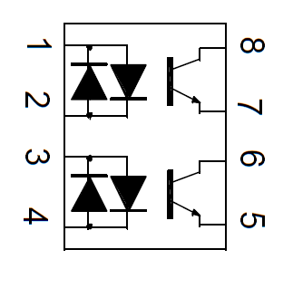
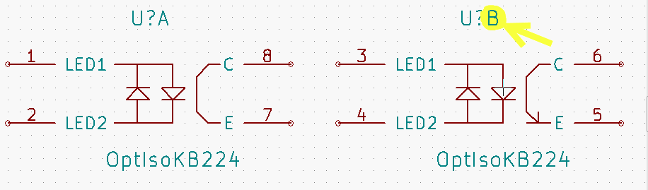
One the left: A diagram of what's in a KB224 dual gate opto-isolator. We're going to create a KiCad component so that we can use KB224's in our design work. A KB224 is a small blob of plastic with 8 legs. Inside it there are TWO independent opto-isolators. (The presence of two LEDs for each means that these opto-isolators not only do the "isolating" implied by the name, but they also take AC signals in, and send a DC signal out.)
Somewhere, someday, I need to address the "simple" case of creating a new component. Today, I am addressing the creation of a "complex" component.
It wouldn't be complex, except for the fact that KiCad (and most other PCB-CAD packages) do something clever: On the schematic, the two modules inside the KB224 can appear in quite separate places.
So how is the component done?
Start KiCad
Start the Schematic Design Editor (eeSchema).
Before vers 5: You would want: Tools/ "Library editor"
Version 5: You want: Tools/ "Symbol library editor"
I don't like either name! But whatever you call it, this is what you want, if you want to edit an existing component, or create a new one (from scratch or by saving a modified version of an old component under a new name).
The "library" editor creates (or merely modifies) the files (.lib and .dcm) of the component. That component becomes available to you when you've made the folder those files are in part of the set of folders "known" to KiCad.
Which folders are "known" is managed...
Before vers 5: Via the eeSchema/ Preferences/ Component Libraries dialog.
Version 5: Via the eeSchema/ Preferences/ Manange Symbol Libraries dialog. (Or use the "Create, delete and edit symbols" tool button.)
(Old, pre ver 5 stuff- this paragraph): Surely "Library Editor" should be "Component Editor"? Ah well. The title for the tool's window (KiCad vers 4-0-4): "Part Library Editor" doesn't seem right to me. The editor is for editing the PARTS (or creating new ones). Yes, you put the parts in .lib files. But would you call a wordprocessor a "folder editor", just because the product of the wordprocessor goes in a folder??
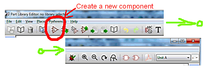
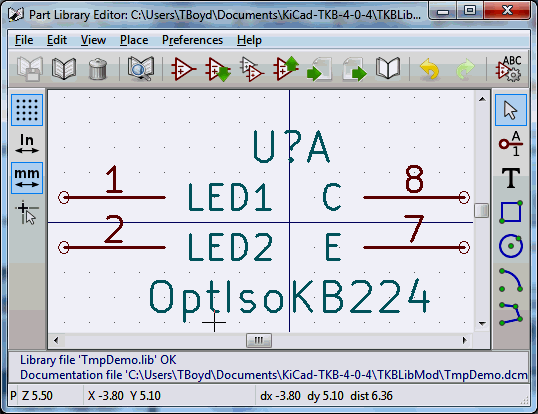
Once the Symbol Editor (... Version 5 name. Previously "Part Library Editor") is up and running, here's what's next.
(The above is the top of the Symbol Editor window, split into two parts, to make it fit the page better. (The graphic is from before KiCad 5, but is close enough to "do".)
If revising an existing part, you start by connecting to the .lib file it is on. If, as we are going to, you are creating a new part, and starting a new .lib file a the same time, you can start with the part, and create the .lib file for it later. (Note that you are unlikely to want to create a separate .lib for each part, but separate .libs can be useful for keeping things organized.
There doesn't seem to be a menu item, for creating a new part. You use the icon indicated, which has "Create a new symbol" for it's tool-tip. (V5... previously "... new component.")
That, vers 4, threw up a dialog... asking you what you wanted to call the component. Under vers 5, you start by saying which library the new component should be put in.
I would strongly advise you NOT to put things you've done in the "system" libraries. Make a library of your own, for your stuff. It, or things in it, may become flawed. Keep it way from the Good Stuff the nice KiCad people gave you. So... if you are on vers 5, cancel out of trying to create a new symbol... for now... and set up a library to hold your symbols....
Happily, setting up your own (symbols) library, and having the things in it routinely available is not difficult. And it is something you only have to do once.
Here begins some "version 5 (and, we hope, above for some time to come!) specific" text. You will be told when we return to a mix of the old and the new.
Using your operating system's ordinary tool (File Explorer, in Windows) create a folder for the symbols you want to add to your KiCad environment.
Now... folder heirarchy design is a huge topic. I have all the "system" files of KiCad in one place, and my KiCad "stuff" in another.
As I said earlier, a main repository of symbol data inside the KiCad system folders is...
\KiCad\share\kicad\library
My initials, "tkb", have not (yet), thankfully, been generally adopted by the industry for anything. So I include them in folder names to help me recognize things created by me, not by "the system". So, in the part of the hard disc where I'm keeping the KiCad stuff I've created, I created a folder called library_tkb_symbols.
Within that, create an empty file with ".lib" as the extension. I called mine aaTKBsymsFrmJan2020.lib
Right! Back to work... having set up that folder and empty, you need to tell KiCad to look there, when creating lists of available symbols.
In KiCad's Symbol Editor, go into "Preferences/ Manage Symbol Libraries". (It is available from other places, too.) That should give you... (vers 5)
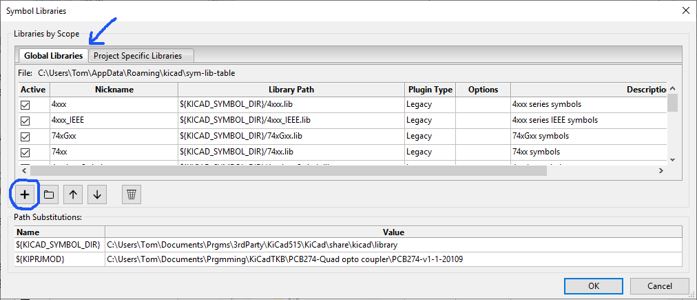
Be sure you are on the "Global Libraries" tab, and then click the "+" near the bottom left, to add a line to the table. This should create a blank line in the table above the "+".
Make up a nickname. In the "Library Path" column, use the folder icon that appears when you select the field to drill down to the .lib file we just created. Leave Plugin type as "Legacy", Options empty. Put a description in.
Click "Okay". You'll get an error message: "Cannot load aliases". That's okay. Your .lib file is empty so far. Click OK again.
Now we are ready to create a new symbol!
In the Symbol Editor, again invoke "Create New Symbol".
Select the symbol library you just created. (This will determine where the symbol gets stored.)
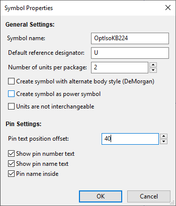
When you've done that, the "Symbols Properties" dialog should appear.
This is the end of the current section of "version 5 specific" text. Hurrah! We are returning to a mix of the old and the new.
Component name...
Call it whatever you like. Make short. I'm using OptIsoKB224. Default reference designator: "U"... fairly common for "chips"... In a given circuit, you'll may have several. They would be referred to as U1, U2, U3, etc. Number of units per package: Two, for the KB224. The others can be left in default states....
Start by placing FOUR (not 8) pins on the screen.
When I do these pages, I "do" what the page says, as I go along. And I "re-do" it when doing a major edit. It has taken 3 hours to get to here, doing a through update to what is true in Version 5. At this point, I may have to start being less fussy. You may have to use more imagination to spot where things under version 5 aren't quite what they were. Sorry.
Having said that, and pressed ahead with reviewing the rest of this page, I discovered major differences between how vers 4 and vers 5 deal with things like the dual opto-coupler that was my example.
In the symbol editor, because we said the component had two units (see Edit/ Properties), in the main Symbol Editor window, there is a pull down allowing use to work on Unit A or Unit B.
Do most of what's needed with that set to Unit A. Then change it to Unit B. Then switch to Unit B. What you've done so far is carried across... you only need to supply the pin numbers, and all comes right! If you, say, draw a line in the symbol for one of the units, it appears on the other one... by default. Right-click on the line, invke "Edit", and you will find a checkbox to make that line not common to all units. Brilliant! Most of the messy stuff below, about creating the second unit on your drawing, won't be needed, if you are on vers 5!
Fill in their properties as you go along, as follows...
Name / Number / Orientation / Electrical type
LED1     1        right         passive
LED2     2        right         passive
C        8        left        open collector
E        7        left        open emitter
As ever... be sure to save your work frequently as you proceed.
m(I also moved th field reference and field value to achieve...)
(Moving things is easy... put pointer over the item you want to move, press "M". Move mouse, item will move. Click to put it down.)
Some details...
The pin names "only" matter to making the component easy to use. LED1, LED2.. the pins which connect to the LEDs inside the opto-isolator. C "Collector", E "Emitter" of photo-transmitter.
Pin numbers: These will be used to match up the "diagrammatic" schematic diagram to the actual physical device to be placed on the PCB... through the "magic" of "CvPCB", with which we "connect" the components in a schematic to the footprints on the PCB. (The device we are creating a component for will go in an 8 pin DIP, remember. For the LEDs in the KB224 which are connected to pins 1 and 2 illuminate the phototransistor connected to pins 7 and 8.
Orientation: This just sets the "direction" of the pin symbol on the component.
Electrical type: The "type" of signal here. To be honest, I don't fully understand the whys and wherefors of this field, yet. I do my best to specify the types correctly. I usually look at a similar KiCad-supplied component, and copy what I see there!
Now we are going to add some lines to the component. They will be a bit approximate. You can make them as fancy, as meticulous as you like. They are to show the engineer what's where, as he works with the component you are creating. I have moved other things about, on the path to the following.
Aside: To drag several elements, together: Drag out a box around them, and then move mouse. Click to "put them down". Only things fully inside the box you dragged out will be included in the group for dragging.
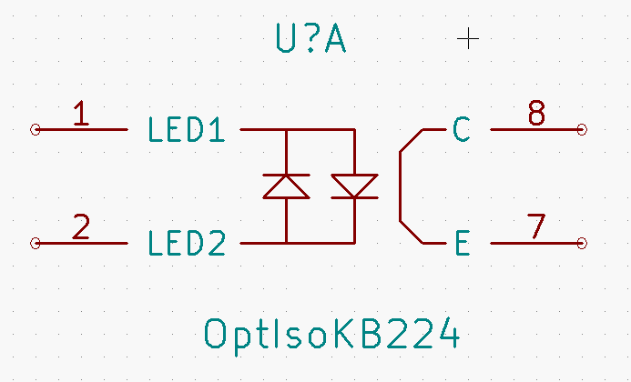
Yes! Something is "wrong"... that is slightly incomplete. (No arrow on the photo-transistor. All will be explained.)
That takes care of what's in the KB224, connected to it's pins 1, 2, 7 and 8. What about the other "unit", the second opto-isolator in the blob of plastic? The one on pins 3,4, 5 and 6?
While doing the schematic, we don't care what pins connect to what things. We don't care that the two opto-isolators in our design are in one package. But when we make the PCB all of that will matter!
There's a trick.
This is the toolbar we saw earlier. See the "Unit A" at the right hand end? If you have re-sized the window, and made it too narrow, you won't see the "Unit A". But we NEED that. Use it to change what we are working on to "Unit B". You should see...
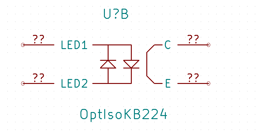
The lines we drew, in connection with Unit A have been shown for unit B, too. (We don't have to re-draw them.) There are "proto-pins" in place... but they need to have various properties set. Go to each in turn, press "E" while the cursor is over the pin. Fill in the pin numbers. The other values will be as before, and they are already filled in for you...
Name / Number / Orientation / Electrical type
LED1     3        right         passive
LED2     4        right         passive
C        5        left        open collector
E        6        left        open emitter
Besides doing that, I have added two small lines, at the bottom right, making an "arrowhead" in the photo-transistor. I have edited each of them to REMOVE the default-provided "tick" against "Common to all units in the component". Don't worry about why I did that, for the moment.
That's it! We've made a component. Now we will use it in a design.
I did a fresh start of KiCad at this point, started new project, and invoked eeSchema.
With "Preferences/ Component Libraries", I told eeSchema that this project would be using the .lib we just created, the one with the component for the KB224 inside it.
I used "Place Component", twice, to get as far as...
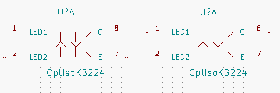
I then right-clicked on the right hand instance of the opto-isolator. Once I had the Component Properties dialog open, I changed the "Unit" from "A" to "B", and NOW what I had in the eeSchema window was...
The top line is now "U?A U?B", whereas it used to be "U?A U?A". (The "?" can be changed by editing the component. "1" would be a sensible number, as there's only one chip in the circuit.)
Notice also that the right hand component HAS the little "arrow" on the photo-transistor, whereas the one on the left does not. In this case, it would have made sense to do the two little lines making the arrow the same way as we made the all other lines. However... sometimes there are multiple units, not all exact clones of one another, inside a chip, and now you've seen how to handle those circumstances.
Just to make the circuit a little more life-like, I added a few bits and pieces....
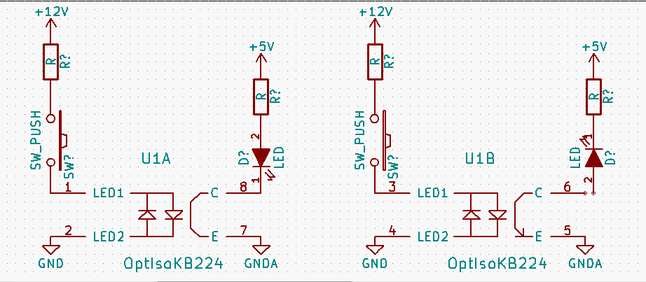
Pretty boring, really. If all we wanted was the schematic, we might as well have just done one unit, and photocopied that.
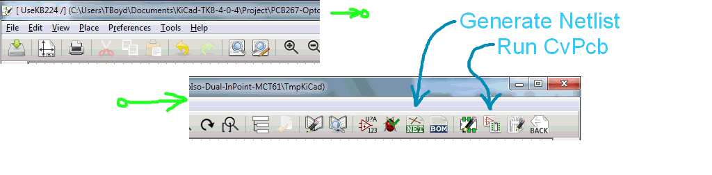
But that's not all we want. Save the netlist (button in top boarder. Allow the "annotation" it will ask to do. Run CvPcb. Most choices are obvious enough... but I had trouble finding the DIL (or DIP) socket, the first time I used 4-0-4. It was under "Power_Integrations:PDIP-8".
And, at last... a PCB design!
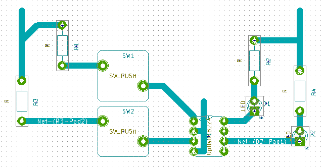
There you have it...
We've created a new component, one with two "units" in it, and created a PCB using one of them.
I hope bits and pieces along the way were useful?
This is at least the second time I've tried to address this topic. For another attempt, see Making and Using Multi-Gate Components
![]() Page has been tested for compliance with INDUSTRY (not MS-only) standards, using the free, publicly accessible validator at validator.w3.org. Mostly passes.
Page has been tested for compliance with INDUSTRY (not MS-only) standards, using the free, publicly accessible validator at validator.w3.org. Mostly passes.
AND passes...

- - - - - Page Ends - - - - -